Cleanroom
Open to all researchers at the university and accessible for external organisations as well, our cleanroom enables wafer-scale micro and nano fabrication. It comprises several class-1000-rated rooms and houses process tools for lithography, dry etch, deposition, chemical processing, post processing and characterisation. These tools are used for rapid prototyping of a range of devices, including photonic structures, microfluidics, micro-lenses, integrated circuits and MEMS. Equipment and specifications listed below.
Lithography
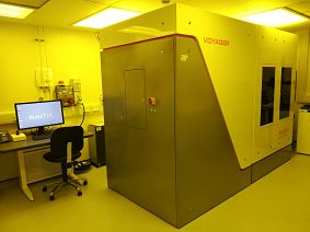
- High performance electron beam lithography tool
- Greater than 1cm²/hr writing speed (at 50 % pattern density)
- 8nm linewidth in HSQ resist
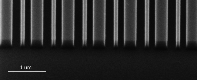
- 30nm pitch grating with 10nm linewidth
- Stitching accuracy <20nm
- Fixed Beam Moving Stage (FBMS) and Modulated Beam Moving Stage (MBMS) patterning modes available (stitching-error-free)
- Linear grating coupler fabricated on SOI wafer
- 3" maximum wafer size
- UV 400 optics
- Standard processes available using S1800 series, LOR, AZ resists
- Sub-micron resolution achievable in vacuum contact mode
- Up to 6" wafer size
- Sub-micron resolution in vacuum contact mode
- Backside alignment using through-wafer IR illumination
- Beam uniformity of 3% across 4" wafer
- 30 kV accelerating voltage
- Raith ELPHY plus patterning system
- 50nm linewidth resolution
- Imaging with tilt and rotation
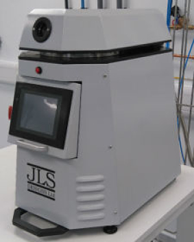
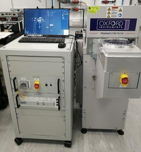
Dry etch
- JLS Designs Plasmapod Plus and Plasmatherm RIE 550-570
- Available for etching SiO2 and Si3N4
- Primarily these system are used to produce hard masks for further wet and dry etching steps
- Other materials have also been etched in the Plasmatherm system, most recently polyimide
- Gases available are CF4, CHF3, Ar, O2
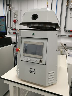
- JLS Designs Plasmapod RIE
- Used for etching silicon and superconducting thin films such as niobium nitride
- Available gases are SF6, CHF3, Ar and O2
- A further two gas lines are currently spare
- Configured for III-V, II-VI etching
- 4" wafer holder
- Up to 8 process gases available that are suitable for etching a wide range of materials, including silicon and LiNbO3
- Standard processes available for high quality InP etching
- Configured for high quality Si etching
- SF6-based etch processes
- Etch recipes for
- RIE, ICP-RIE
- Bosch
- Cryo
- 4" wafer holder, can be configured for up to 8"
- Laser end-point detection
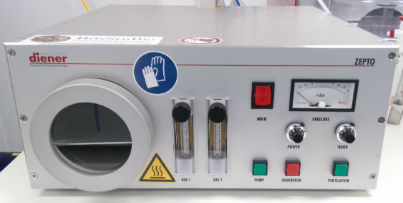
- O2 and Ar plasma asher
- Surface functionalisation and sample cleaning
- 105mm diameter chamber
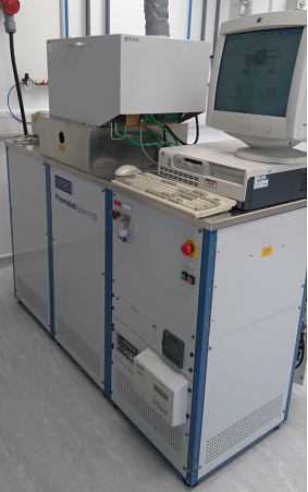
Deposition
- Three targets, 2" diameter - Au, NiCr, Ti, Pd, Pt available and other materials by request
- Rotational sample holder
- Confocal or parallel sputter head orientation
- Better than +/- 5% uniformity across 4" wafer (confocal deposition)
- Metal deposition - Au, Ni, Ag, Al, Cr, other metals by request
- Thin films, usually < 300 nm
- Base pressure typically 1.10-6 mbar
- a-Si, SiO2 and Si3N4 deposition
- Loadlocked system
- Ammonia-free Si3N4 recipes available
- Metal deposition: Au, Ti, Al, others by request
- Dielectric material deposition: Al2O3, SiO2
- Six-pocket e-beam gun with 7 cc volume
- Integrated into sputter coater system
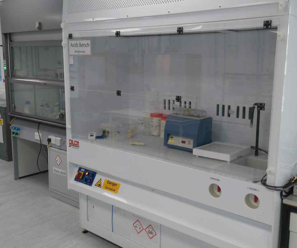
Chemical processing
- Acid/base processing
- HF processing
- Solvent cleaning
- Spin station (photoresists)
- Spin station (coating system for SU-8 and spin coater for EBL resists)
- Transene TFA Au etch
- Transene TFG Ni etch
-
Transene TFN NiCr etch
-
Aqua regia
-
Piranha
-
HF/BOE
Post processing
- Eutectic die bonder
- Precision placement
- Vacuum pick and place
- 4" wafer compatible
- Variety of cutting modes
- Single and multi pass
- Programmable rotation with 0.005° resolution
- Square, circular, hexagonal substrates, up to 8 mm thick
- Servo-driven y-axis with 2 μm resolution
- Feed-rate from 0.1 mm/sec upwards
- Spindle speed from 3000-40000 rpm
- Precision diamond scribing
- Optical alignment
- 3" wafer vacuum chuck
- Gold ball bonding
- 25um diameter wire
- Fine pitch capillaries available
- Gold ball and wedge bonding (25um diameter as standard)
-
Aluminium wedge bonding (33um diameter as standard)
-
17-50um diameter wire bonding possible
-
Fine pitch capillaries available
-
Loop control
-
Manual, semiautomatic, automatic bonding
Characterisation
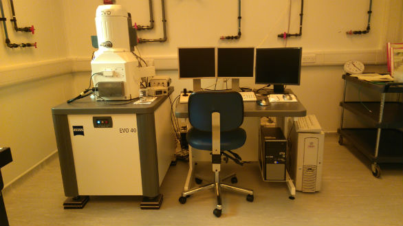
- SEM used for surface characterisation and imaging
- 5-30kV accelerating voltage
- Primarily a patterning tool, but available for some imaging purposes
- Variable pressure mode available
- High precision, scientific-grade microscope, providing atomic-scale resolution
- Applications in material science, polymers and general surface characterisation
- Contact and Intermittent contact AFM modes available
- Stylus with 2 μm diameter tip
- 3D profilometer
- Step height repeatability of 4 Å possible
- Vertical size limit of 1 mm
- 6" wafer compatible
-
High quality measurement of thin film and bulk characteristics including
- Optical dispersion (complex refractive index, dielectric permittivity)
- Film thickness
- Multi-layer characterisation
- Films may be isotropic or anisotropic, homogenous or graded
- Wide wavelength range: 210-2500 nm
- Variable angle: 45-90 degrees
- Interferomtric white light profilometer
- Measures surface profiles with vertical feature resolution down to 0.001 µm by using white light interferometry (WLI)
- Automated XY stage
- Two objective lenses
- 20x : field of view = 1.0 x 0.85 mm (spatial sampling = 0.44 um)
- 100x : field of view = 0.2 x 0.17 mm (spatial sampling = 0.088 um)
- Quick and easy thin film thickness measurement
- Wafers up to 6"
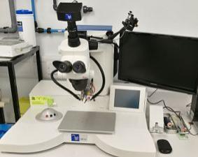
- Variety of inspection microscopes available
- Polyvar Polymet microscope fitted with objectives ranging from x2.5 to x150 calibrated to permit length measurements
- Leica viewers and inspection microscopes also available